With the increasing demands of consumers, 3D integrated circuits are a crucial component for improving the efficiency of electronics. However, despite constant development, it is difficult to turn theoretical findings into actual devices. A team of researchers from the Institute of Industrial Science at The University of Tokyo, Japan has developed a new design that can translate theoretical findings into reality.
New Deposition Process for Nanosheet Oxide Semiconductor
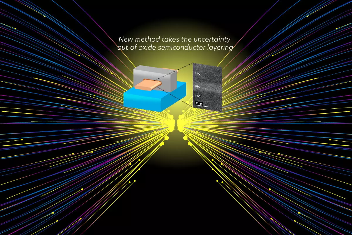
The researchers have published a study on their new design in the VLSI Symposium 2023. They have developed a deposition process for nanosheet oxide semiconductor that has high carrier mobility and reliability in transistors. 3D integrated circuits consist of multiple layers that each play a role in the overall function. Oxide semiconductors are becoming popular materials for various circuit components as they can be processed at low temperatures, have high carrier mobility and low charge leakage, and can withstand high voltages. Using oxides instead of metals in processes where electrodes may be exposed to oxygen during the integration process has its advantages because they do not get oxidized.
However, developing the processes for depositing very thin layers of oxide semiconductor materials in the manufacture of devices is challenging and has not been fully established to date. The researchers have reported an atomic layer deposition (ALD) technique that produces layers appropriate for large-scale integration. They carried out a systematic study of field effect transistors (FETs) using their process to establish their limitations and optimize their properties. FETs control the current flow in a semiconductor. They tuned the ratio of the components and adjusted the preparation conditions to develop a multi-gate nanosheet FET for normally-off operation and high reliability.
High Performance FETs
Their findings showed that a FET made from the chosen oxide semiconductor by ALD had the best performance. The multi-gate nanosheet FET is believed to be the first to combine high carrier mobility and reliability characteristics with normally-off operation. The lead author of the study, Kaito Hikake, says, “Using our process, we carried out a systematic study of field effect transistors (FETs) to establish their limitations and optimize their properties. We tuned the ratio of the components and adjusted the preparation conditions, and our findings led to the development of a multi-gate nanosheet FET for normally-off operation and high reliability.”
The senior author, Masaharu Kobayashi, explains that in rapidly moving areas such as electronics, it is important to translate proof of concept findings into industrially relevant processes. He believes that their study provides a robust technique that can produce devices that meet the market’s need for manufacturable 3D integrated circuits with high function.
The new design by the Japanese research team has developed a deposition process for nanosheet oxide semiconductor that has high carrier mobility and reliability in transistors. The atomic layer deposition (ALD) technique produces layers appropriate for large-scale integration, making it possible to develop high-performance multi-gate nanosheet FETs. This is a significant development as it provides a solution to one of the big obstacles in the manufacturing of electronic devices with semiconductors. This new design could lead to more designs of electronics with high functionality being developed into actual products.
Leave a Reply